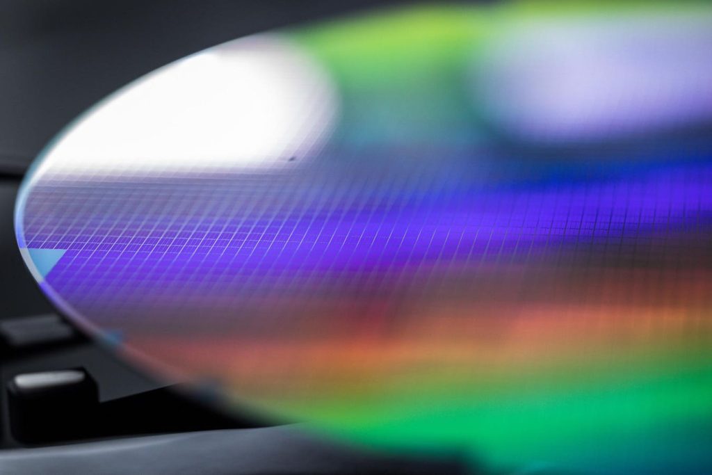
In this article we look at the Lam Research Coronus DX edge bevel deposition announcement to increase yield of semiconductor wafers after complex processes, such as during the creation of 3D NAND. Also, SEMI, the semiconductor equipment trade association, projects growth in 300mm wafer fab equipment demand in 2024 and 2025 following a decline in 2023.
Deposition equipment is key to making modern solid state memory devices. Various thin film processes are needed to deposit and etch the various layers. As the number of 3D NAND layers increases the production process time generally increases and the opportunities to damage the edge of the wafer increase with the number of operations. Repeated layers of processing can cause residues and roughness to accumulate along the wafer edge where they may flake off, drift to other areas, and create defects that cause a semiconductor device to fail.
Long wet etch processes in 3D NAND manufacturing may result in severe substrate damage at the edge. Also, in 3D packaging, material from back-end-of-line can migrate and become a contamination source in future processing. In addition, erosion of the wafer edge can reduce the quality of wafer-to-wafer bonding.
This week Lam Research introduced the company’s Coronus DX bevel deposition solution to reduce damage and contamination on the edge of the silicon semiconductor substrates as shown below.
In a single step, Coronus DX deposits a thin dielectric layer of protection on the bevel. This precise and tunable deposition helps resolve these common issues that impact semiconductor quality. This protective layer increases yield and enables chipmakers to implement new leading-edge processes for the production of next-generation chips, including 3D NAND. The image below shows the Coronus deposition apparatus.
According to the company, Coronus DX enables best-in-class precision wafer centering and process control, including integrated metrology, to ensure consistency and repeatability of the process. Coronus products incrementally increase wafer yield, delivering an additional 0.2 to 0.5 percent of yield per etch or deposition step, which can result in up to 5 percent improvement across the wafer workflow. Manufacturers running more than 100,000 wafer starts per month may yield millions of extra die with Coronus – potentially worth millions of dollars – over the course of a year.
Coronus DX is the newest addition to the Lam Research Coronus product family. Lam’s Coronus is used by every major chipmaker.
Things may be looking up for semiconductor equipment manufacturers and the companies that use their equipment to make semiconductors that power almost every aspect of modern life. SEMI, the semiconductor equipment industry trade group reports that Global 300mm fab equipment spending for front-end facilities next year is expected to begin a growth streak to a US$119 billion record high in 2026 following a decline in 2023, SEMI highlighted today in its quarterly 300mm Fab Outlook Report to 2026 (see figure from the SEMI press release below).
SEMI says that strong demand for high-performance computing, automotive applications and improved demand for memory will fuel double-digit spending in equipment investments over the three-year period.
SEMI says that strong demand for high-performance computing, automotive applications and improved demand for memory will fuel double-digit spending in equipment investments over the three-year period.
Korea is expected to lead global 300mm fab equipment spending in 2026 with US$30.2 billion in investments, nearly doubling from US$15.7 billion in 2023. Taiwan is forecast to invest US$23.8 billion in 2026, up from US$22.4 billion this year, and China is projected to log US$16.1 billion in spending in 2026, an increase from US$14.9 billion in 2023. Americas equipment spending is expected to nearly double from US$9.6 billion this year to US$18.8 billion in 2026.
Foundry is projected to lead other segments in equipment spending at US$62.1 billion in 2026, an increase from US$44.6 billion in 2023, followed by memory at US$42.9 billion, a 170% increase from 2023. Analog spending is forecast to increase from US$5 billion this year to US$6.2 billion in 2026. The microprocessor/microcontroller, discrete (mainly power devices), and optoelectronics segments are expected to see spending declines in 2026, while investments in logic is forecast to rise.
LAM Research introduces its Coronus DX semiconductor bevel edge deposition technology to increase yield for complex processes such as in 3D NAND. SEMI projects growth in 300mm wafer fab equipment spending in 2024 and 2025 after an 18% decline in 2023.
Read the full article here


